T H E M A G A Z I N E F O R T H E P H O T O N I C S & O P T O E L E C T R O N I C S I N D U S T RY
®
AUGUST 2005
W W W. L A S E R F O C U S W O R L D . C O M
Disk lasers redefine
diode pumping
Spectrophotometry
characterizes OLEDs
Fiber lasers push up
the power
Optics expand
ultrafast applications
SPECIAL REPORT
Tiny tech
makes
big business
➤ PAGE 121
Manufacturers’
Product Showcase
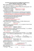
THIN-FILM METROLOGY
Reflection, transmission
spectrophotometry
characterizes
OLED materials
–
V
+
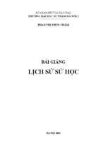
CHRIS CLAYPOOL
Electron-transport layer
(e.g. Alq3)
Light-emitting layer
(e.g. Doped Alq3)
Hole-transport layer
(e.g. NPB)
Indium tin oxide
T
Glass
he spectacular growth of the organic-lightemitting-device (OLED) industry over the
Electroluminescent light
past couple of years has highlighted the
technical challenges faced in the manufacFIGURE 1. Electroluminescent light is produced in an organic lightturing of these devices. The accuracy, repeat- emitting device when electrons and holes recombine in the lightability, and uniformity of the organic-layer thicknesses is
emission layer. The accuracy, repeatability, and uniformity of the
a critical manufacturing issue for OLED displays because organic film thicknesses are important manufacturing issues to
which reflection and transmission spectroscopy can be applied.
these parameters directly affect the brightness and color
uniformity of pixels in the display. Furthermore, knowledge of the optical properties of An advanced metrology tool
optical constants (refracthe organic layers is necessary for optimizing
tive index n and extincthe design of the OLED display, including
tion coefficient k). These
characterizes multilayer
the design of microcavities, and in undertechniques, however, have
thin-film OLED structures
standing device properties such as external
limitations when applied
light-coupling efficiency. Reflection and
to OLED-related applicabased on power-spectraltransmission spectrophotometry is a fast,
tions in which the organic
noncontact, and nondestructive characterfilms of interest tend to be
ization method that is ideally suited for these density analysis of
thin and highly absorbing
OLED manufacturing challenges.
in the UV range and are
spectroscopic multiangle
deposited on transparContending with OLED absorption polarized reflection, polarized ent substrates. Although
Optical-metrology methods, including
reflectometry (reflecreflectometry and spectroscopic ellipsometry, transmission, and spectrotion spectrophotometry)
have found widespread use in the silicon inmethods can readily descopic ellipsometric data.
dustry for monitoring layer thicknesses and
termine film thickness (t)
if the optical constants of
the film are known (fixed), the technique does not inherentCHRIS CLAYPOOL is chief technical officer of Scientific Computing
ly contain enough measured information to solve n, k, and t
International, 6355 Corte Del Abeto, Suite C-105, Carlsbad, CA 92009;
e-mail:
[email protected]; www.scie-soft.com.
of the film independently.
108
August 2005 www.laserfocusworld.com
Laser Focus World
System design
We have developed advanced metrology
tools based on a new optical technique
that uses power-spectral-density analysis of spectroscopic multiangle polarized
reflection, polarized transmission, and
spectroscopic ellipsometric data. For the
purpose of analyzing the OLED samples
described here, we have limited our analysis to normal-incident spectroscopic reflection and transmission data. We have
found that this method allows for fast
and accurate material analysis and thickness determination of films during the
production of OLED devices.
The instrument (called the FilmTek
3000) used to measure and analyze the
100
80
60
40
ITO thickness =
1656.2 Å
20
0
200
400
600
800
Wavelength (nm)
1000
80
60
40
Doped Alq3 thickness =
217.1 Å
20
0
200
400
600
800
Wavelength (nm)
1000
% Reflection/transmission
100
Measured %T
Measured %R
100
% Reflection/transmission
% Reflection/transmission
Simulated %T
Simulated %R
% Reflection/transmission
Spectroscopic ellipsometry, on the
other hand, measures the polarization
states of collimated monochromatic light
before and after reflection from a surface
to obtain the ratio of the complex p- and
s-polarization reflection coefficients and
provides twice as much information in
the experimental data as does reflectometry; however, accurate determination of
the extinction coefficient can be difficult
without transmission data.
As a result, slightly more-involved
analysis, such as the use of multiple sample data sets and/or determining thickness first in a nonabsorbing wavelength
region, may be necessary to arrive at a
unique solution for n, k, and t. The partial
reflection from the backside of the transparent OLED substrate and the birefringence of some polymer OLED substrates
(for example, polyethylene terephthalate
films) adds additional complexity to the
collection and analysis of spectroscopic ellipsometric data for OLED applications. Although these two unknown effects can be incorporated in the optical
model, they introduce uncertainty in the
uniqueness of the solution of the optical
parameters.
Alternatively, transmission spectrophotometry is an ideal technique for
measuring absorption and provides better resolution of the film’s extinction
coefficient compared with spectroscopic ellipsometry. Combining reflection
and transmission spectrophotometry in
a single instrument provides two data
sets with enough information content to
uniquely determine the thickness and optical constants of thin absorbing films on
transparent substrates.
100
80
60
40
NPB thickness =
437.9 Å
20
0
200
400
600
800
Wavelength (nm)
1000
80
60
40
Alq3 thickness =
244.8 Å
20
0
200
400
600
800
Wavelength (nm)
1000
FIGURE 2. The modeled reflection and transmission spectra of single-layer OLED films on
glass are in good agreement with measured data. The OLED layer thicknesses and optical
constants are determined simultaneously. By using a general dispersion model that covers the entire wavelength range of the measurement, the number of parameters required to
model optical response is reduced, eliminating the potential for multiple solutions.
OLED samples is a fiber-based system
with a tungsten-deuterium light source
and fixed-grating CCD-array spectrometers. Absolute reflection and transmission spectra are obtained by collecting
reflection and transmission spectra from
ANALYSIS OF THE
REFLECTION AND
TRANSMISSION DATA
GIVES ACCURATE
THICKNESS VALUES
AS WELL AS THE
REFRACTIVE INDEX
AND EXTINCTION
COEFFICIENTS.
the sample of interest in ratio to reflection
and transmission spectra from known
samples (bare silicon for reflection and
air for transmission). Reflection and
transmission spectra can be measured
from the deep-UV to near-IR, with acquisition time taking a fraction of a secLaser Focus World
ond. Various optical configurations allow
for a measurement spot size that ranges
from 3.5 mm to 2 µm.
Accompanying soft ware simultaneously solves for refractive index n(λ),
extinction coefficient k(λ), and thicknesses of multilayer fi lm structures. A
self-consistent solution is obtained by
using a generalized dispersion formula developed at Scientific Computing
International to model fitted values
of the dielectric function ε(λ) to the
measured reflection and transmission
data. The dispersion formula is a selfconsistent model that is derived from
quantum-mechanical principles and
correctly obeys the Kramer-Kronig relationship. It is applicable to metallic,
semiconductor, amorphous, crystalline, dielectric, and organic materials.
By using a general dispersion model
that covers the entire wavelength range
of the measurement, the number of variables or parameters required to model
optical response is reduced, eliminating
the potential for multiple solutions. This
approach allows the user to model complex multilayer structures with reflection
and transmission data. Global-optimizawww.laserfocusworld.com
August 2005
109
1.8
1.6
1.4
1.2
200
k
400 600 800 1000
Wavelength (nm)
Index of refraction (n)
2.5
1.2
Doped Alq3
optical
properties
2.3
2.1
1.9
n
1.7
1.5
1.3
200
k
400 600 800 1000
Wavelength (nm)
1.0
0.8
0.6
0.4
0.2
0.0
-0.2
2.0
0.3
1.9
1.6
200
0.2
n
1.8
1.7
0.1
k
0.0
400 600 800 1000
Wavelength (nm)
Alq3 optical
properties
2.3
2.1
1.0
0.8
0.6
1.9
n
1.7
1.3
200
-0.1
1.2
2.5
1.5
0.4
k
400 600 800 1000
Wavelength (nm)
0.4
0.2
0.0
-0.1
Extinction coefficient (k)
n
NPB optical
properties
2.1
Extinction coefficient (k)
2.0
Index of refraction (n)
2.2
0.5
2.2
Index of refraction (n)
ITO optical
properties
2.4
0.7
0.6
0.5
0.4
0.3
0.2
0.1
0.0
-0.1
Extinction coefficient (k)
Index of refraction (n)
2.6
Extinction coefficient (k)
THIN-FILM METROLOGY, continued
FIGURE 3. Fitted optical constants are determined from analysis of the reflection and
transmission spectra obtained from single-layer OLED films on glass.
In routine use
Reflection and transmission spectrophotometry is a powerful technique for characterizing the organic-film thicknesses
and optical constants of multilayer OLED
thin-film structures. The FilmTek 3000
is routinely used for the noncontact optical characterization of multilayer OLED
structures on glass substrates. In one example, the reflection and transmission
spectra of single-layer OLED films on
glass are obtained from 240
to 1000 nm (Fig. 2). Analysis
Simulated %T
Measured %T
Application to OLED
of the reflection and transSimulated %R
Measured %R
thin-film structures
mission data gives accurate
100
Alq3
Light is produced in OLEDs
thickness values as well as
252.2 Å
80
when an appropriate voltthe refractive index and exDoped Alq3 201.3 Å
age is applied across the
tinction coefficients over the
60
448.6 Å
NPB
electrodes, causing elecsame wavelength range (see
1574.2 Å
ITO
40
trons and holes to recomFig. 3). The layer thicknesses
Glass
bine in the light-emission
of a multilayer OLED struc20
layer (electroluminescence).
ture on glass can also be de0
200
400
600
800
1000
The most commonly used
termined accurately and siWavelength (nm)
emitter material is tris (8multaneously (see Fig. 4).
hydroxyquinoline) alumi- FIGURE 4. The modeled reflection and transmission spectra of a multiWhen reflection and
num (Alq3). Changing the layer OLED film stack on glass are in good agreement with the meatransmission spectrocomposition of the organic sured data. The multiple OLED layer thicknesses can be determined
photometry is used for
layers tunes the OLED
simultaneously, with combined measurement and analysis time of one high-throughput large-area
emission colors across the to two seconds per point.
flat-panel-display applicavisible spectrum. For extions, large custom stages
ture about 1000 to 2000 Å thick (see Fig. and small measurement-spot sizes allow
ample, by doping the Alq3 layer with
other organic molecules, energy trans- 1). Small-molecule OLEDs are deposited the simultaneous determination of layer
under vacuum by thermal sublimation,
fer from the Alq3 to the dopant results
thicknesses and optical properties—key
while polymer-based OLED fi lms are
in lower energy (redder) emission.
performance metrics in the manufacAlso, substantial shift s in the electrolu- spin-coated and heat-treated. The subture of OLEDs.
❏
minescent wavelength can be achieved
by controlling the number and chemical nature of the quinolate ligands in
Alq3. With these approaches, devices
with electroluminescent emission in
the red, green, and blue spectral regions have been demonstrated.
A typical OLED structure consists of
organic layers grown on a glass or plastic substrate to form a multilayer struc-
% Reflection
tion methods are used to obtain the best
solution while avoiding local minima and
minimizing sensitivity to the user’s initial
guess of fitted parameters (for example,
layer thickness). The software optimizes
the reflection, transmission, and the power-density-spectrum (fast-Fourier-transform) data simultaneously. This allows for
accurate thickness determination over a
wide range of thicknesses from 3 nm to
350 µm.
strate is first coated with a conducting transparent electrode such as indium tin oxide (ITO), which serves as
the anode. This layer is followed by a
hole-transporting layer (HTL) such as
napthylphenylbiphenyl (NPB). An organic light-emitting layer (EML), such
as doped Alq3, is then deposited on the
HTL surface. A similar material is often
used for the electron-transporting layer
(ETL) that is deposited on the EML
surface. The device is completed by depositing a low-work-function metal
cathode such as magnesium-silver alloy.
The optical properties of OLED materials are essentially dependent on their
complex dielectric functions, which are
related to the refractive index n and extinction coefficient k. The nature and
thickness of the organic layers in the
OLED structure can be optimized for
efficient charge migration, recombination, and light emission.
110
August 2005 www.laserfocusworld.com
Laser Focus World