~
~~
~
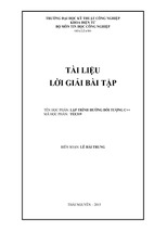
RTL HARDWARE DESIGN
USING VHDL
Coding for Efficiency, Portability,
and Scalability
PONG P.CHU
Cleveland State University
A JOHN WlLEY & SONS, INC., PUBLICATION
~~
~
This Page Intentionally Left Blank
RTL HARDWARE DESIGN
USING VHDL
This Page Intentionally Left Blank
~
~~
~
RTL HARDWARE DESIGN
USING VHDL
Coding for Efficiency, Portability,
and Scalability
PONG P.CHU
Cleveland State University
A JOHN WlLEY & SONS, INC., PUBLICATION
~~
~
Copyright 02006 by John Wiley & Sons, Inc. All rights reserved.
Published by John Wiley & Sons, Inc., Hoboken, New Jersey.
Published simultaneouslyin Canada.
No part of this publication may be reproduced, stored in a retrieval system, or transmitted in any form
or by any means, electronic, mechanical, photocopying, recording, scanning, or otherwise, except as
permitted under Section 107 or 108 of the 1976 United States Copyright Act, without either the prior
written permission of the Publisher, or authorization through payment of the appropriate per-copy fee to
the Copyright Clearance Center, Inc., 222 Rosewood Drive, Danvers, MA 01923, (978) 750-8400, fax
(978) 750-4470, or on the web at www.copyright.com.Requests to the Publisher for permission should
be addressed to the Permissions Department, John Wiley & Sons, Inc., 1 11 River Street, Hoboken, NJ
07030, (201) 748-6011, fax (201) 748-6008, or online at http://www.wiley.com/go/pennission.
Limit of LiabilityiDisclaimerof Warranty: While the publisher and author have used their best efforts in
preparing this book, they make no representations or warranties with respect to the accuracy or
completeness of the contents of this book and specifically disclaim any implied warranties of
merchantabilityor fitness for a particular purpose. No warranty may be created or extended by sales
representatives or written sales materials. The advice and strategies contained herein may not be
suitable for your situation.You should consult with a professional where appropriate.Neither the
publisher nor author shall be liable for any loss of profit or any other commercial damages, including
but not limited to special, incidental, consequential, or other damages.
For general information on OUT other products and services or for technical support, please contact OUT
Customer Care Department within the United States at (800) 762-2974, outside the United States at
(317) 572-3993 or fax (317) 572-4002.
Wiley also publishes its books in a variety of electronic formats. Some content that appears in print may
not be available in electronic format. For information about Wiley products, visit our web site at
www.wiley.com.
Library of Congress Cataloging-in-Publication Data:
Chu, Pong P., 1959RTL hardware design using VHDL I by Pong P. Chu.
p. cm.
Includes bibliographical references and index.
“A Wiley-Intersciencepublication.”
ISBN-13: 978-0-471-72092-8 (alk. paper)
ISBN-10: 0-471-72092-5 (alk. paper)
1. Digital electronics-Data processing. 2. VHDL (Computer hardware description
language). I. Title.
TK7868.D5C462006
621.39‘2-4~22
Printed in the United States of America.
10987654321
2005054234
To my parents Chia-Chi and Chi-Te, my wife Lee, and my daughter Patricia
This Page Intentionally Left Blank
CONTENTS
Preface
Acknowledgments
1 Introduction to Digital System Design
Introduction
Device technologies
1.2.1 Fabrication of an IC
1.2.2 Classification of device technologies
1.2.3 Comparison of technologies
1.3 System representation
1.4 Levels of Abstraction
1.4.1 Transistor-level abstraction
1.4.2 Gate-level abstraction
1.4.3 Register-transfer-level(RT-level) abstraction
1.4.4 Processor-level abstraction
1.5 Development tasks and EDA software
1.5.1 Synthesis
1 S . 2 Physical design
1 S.3 Verification
1S . 4 Testing
1.5.5 EDA software and its limitations
1.1
1.2
xix
xxiii
1
1
2
2
2
5
8
9
10
10
11
12
12
13
14
14
16
16
vil
V\i\
CONTENTS
1.6
Development flow
1.6.1 Flow of a medium-sized design targeting FPGA
1.6.2 Flow of a large design targeting FPGA
1.6.3 Flow of a large design targeting ASIC
1.7 Overview of the book
1.7.1 Scope
1.7.2 Goal
1.8 Bibliographic notes
Problems
2 Overview of Hardware Description Languages
2.1
Hardware description languages
2.1.1 Limitations of traditional programming languages
2.1.2 Use of an HDL program
2.1.3 Design of a modem HDL
2.1.4 VHDL
2.2 Basic VHDL concept via an example
2.2.1 General description
2.2.2 Structural description
2.2.3 Abstract behavioral description
2.2.4 Testbench
2.2.5 Configuration
2.3 VHDL in development flow
2.3.1 Scope of VHDL
2.3.2 Coding for synthesis
2.4 Bibliographic notes
Problems
3 Basic Language Constructs of VHDL
3.1
3.2
Introduction
Skeleton of a basic VHDL program
3.2.1 Example of a VHDL program
3.2.2 Entity declaration
3.2.3 Architecture body
3.2.4 Design unit and library
3.2.5 Processing of VHDL code
3.3 Lexical elements and program format
3.3,l Lexical elements
3.3.2 VHDL program format
3.4 Objects
3.5 Data types and operators
17
17
19
19
20
20
20
21
22
23
23
23
24
25
25
26
27
30
33
35
37
38
38
40
40
41
43
43
44
44
44
46
46
47
47
47
49
51
53
CONTENTS
IX
3.5.1 Predefined data types in VHDL
3.5.2 Data types in the IEEE stdlogic-1164 package
3.5.3 Operators over an array data type
3.5.4 Data types in the IEEE numeric-std package
3.5.5 The stdlogic-arith and related packages
Synthesis guidelines
3.6.1 Guidelines for general VHDL
3.6.2 Guidelines for VHDL formatting
Bibliographicnotes
Problems
65
65
66
66
66
4 Concurrent Signal Assignment Statements of VHDL
69
3.6
3.7
4.1
4.2
4.3
4.4
4.5
4.6
4.7
Combinationalversus sequential circuits
Simple signal assignment statement
4.2.1 Syntax and examples
4.2.2 Conceptual implementation
4.2.3 Signal assignment statement with a closed feedback loop
Conditional signal assignment statement
4.3.1 Syntax and examples
4.3.2 Conceptual implementation
4.3.3 Detailed implementationexamples
Selected signal assignment statement
4.4.1 Syntax and examples
4.4.2 Conceptual implementation
4.4.3 Detailed implementationexamples
Conditionalsignal assignment statementversus selected signal assignment
statement
4.5.1 Conversion between conditional signal assignment and selected
signal assignment statements
4.5.2 Comparison between conditional signal assignment and selected
signal assignment statements
Synthesis guidelines
Bibliographic notes
Problems
5 Sequential Statements of VHDL
5.1
5.2
VHDL process
5.1.1 Introduction
5.1.2 Process with a sensitivity list
5.1.3 Process with a wait statement
Sequential signal assignment statement
53
56
58
60
64
69
70
70
70
71
72
72
76
78
85
85
88
90
93
93
94
95
95
95
97
97
97
98
99
100
X
CONTENTS
Variable assignment statement
If statement
5.4.1 Syntax and examples
5.4.2 Comparison to a conditional signal assignment statement
5.4.3 Incomplete branch and incomplete signal assignment
5.4.4 Conceptual implementation
5.4.5 Cascading single-branchedif statements
5.5 Case statement
5.5.1 Syntax and examples
5.5.2 Comparison to a selected signal assignment statement
5.5.3 Incomplete signal assignment
5.5.4 Conceptual implementation
5.6 Simple for loop statement
5.6.1 Syntax
5.6.2 Examples
5.6.3 Conceptual implementation
5.7 Synthesis of sequential statements
5.8 Synthesis guidelines
5.8.1 Guidelines for using sequential statements
5.8.2 Guidelines for combinational circuits
5.9 Bibliographic notes
Problems
5.3
5.4
6 Synthesis Of VHDL Code
6.1
Fundamental limitations of EDA software
Computability
Computation complexity
Limitations of EDA software
Realization of VHDL operators
6.2.1 Realization of logical operators
6.2.2 Realization of relational operators
6.2.3 Realization of addition operators
6.2.4 Synthesis support for other operators
6.2.5 Realization of an operator with constant operands
6.2.6 An example implementation
Realization of VHDL data types
6.3.1 Use of the std-logic data type
6.3.2 Use and realization of the ’Z’value
6.3.3 Use of the ’-’ value
VHDL synthesis flow
6.4.1 RT-level synthesis
6.4.2 Module generator
6.1.1
6.1.2
6.1.3
6.2
6.3
6.4
101
103
103
105
107
109
110
112
112
114
115
116
118
118
118
119
120
120
120
121
121
121
125
125
126
126
128
129
129
129
130
130
130
131
133
133
133
137
139
139
141
CONTENTS
6.4.3 Logic synthesis
6.4.4 Technology mapping
6.4.5 Effective use of synthesis software
6.5 Timing considerations
6.5.1 Propagation delay
6.5.2 Synthesis with timing constraints
6.5.3 Timing hazards
6.5.4 Delay-sensitive design and its dangers
6.6 Synthesis guidelines
6.7 Bibliographic notes
Problems
7 Combinational Circuit Design: Practice
7.1
7.2
7.3
7.4
7.5
7.6
7.7
Derivation of efficient HDL description
Operator sharing
7.2.1 Sharing example 1
7.2.2 Sharing example 2
7.2.3 Sharing example 3
7.2.4 Sharing example 4
7.2.5 Summary
Functionality sharing
7.3.1 Addition-subtraction circuit
7.3.2 Signed-unsigned dual-mode comparator
7.3.3 Difference circuit
7.3.4 Full comparator
7.3.5 Three-function barrel shifter
Layout-related circuits
7.4.1 Reduced-xor circuit
7.4.2 Reduced-xor-vector circuit
7.4.3 Tree priority encoder
7.4.4 Barrel shifter revisited
General circuits
7.5.1 Gray code incrementor
7.5.2 Programmable priority encoder
7.5.3 Signed addition with status
7.5.4 Combinational adder-based multiplier
7.5.5 Hamming distance circuit
Synthesis guidelines
Bibliographic notes
Problems
8 Sequential Circuit Design: Principle
Xi
142
143
148
149
150
154
156
158
160
160
160
163
163
164
165
166
168
169
170
170
171
173
175
177
178
180
181
183
187
192
196
196
199
20 1
203
206
208
208
208
213
CONTENTS
Xii
Overview of sequential circuits
8.1.1 Sequential versus combinational circuits
8.1.2 Basic memory elements
8.1.3 Synchronous versus asynchronouscircuits
8.2 Synchronous circuits
8.2.1 Basic model of a synchronous circuit
8.2.2 Synchronous circuits and design automation
8.2.3 m e s of synchronous circuits
8.3 Danger of synthesis that uses primitive gates
8.4 Inference of basic memory elements
8.4.1 D latch
8.4.2 DFF
8.4.3 Register
8.4.4 RAM
8.5 Simple design examples
8.5.1 Other types of FFs
8.5.2 Shift register
8.5.3 Arbitrary-sequence counter
8.5.4 Binary counter
8.5.5 Decade counter
8.5.6 Programmablemod-rn counter
8.6 Timing analysis of a synchronous sequential circuit
8.6.1 Synchronized versus unsynchronized input
8.6.2 Setup time violation and maximal clock rate
8.6.3 Hold time violation
8.6.4 Output-related timing considerations
8.6.5 Input-related timing considerations
8.7 Alternative one-segment coding style
8.7.1 Examples of one-segmentcode
8.7.2 Summary
8.8 Use of variables in sequential circuit description
8.9 Synthesis of sequential circuits
8.10 Synthesis guidelines
8.1 1 Bibliographic notes
Problems
8.1
9 Sequential Circuit Design: Practice
9.1
9.2
Poor design practices and their remedies
9.1.1 Misuse of asynchronous signals
9.1.2 Misuse of gated clocks
9.1.3 Misuse of derived clocks
Counters
213
213
214
216
217
217
218
219
219
221
22 1
222
225
225
226
226
229
232
233
236
237
239
239
240
243
243
244
245
245
250
250
253
253
253
254
257
257
258
260
262
265
CONTENTS
9.2.1 Gray counter
9.2.2 Ring counter
9.2.3 LFSR (linear feedback shift register)
9.2.4 Decimal counter
9.2.5 Pulse width modulation circuit
9.3 Registers as temporary storage
9.3.1 Register file
9.3.2 Register-based synchronousFIFO buffer
9.3.3 Register-based content addressable memory
9.4 Pipelined design
9.4.1 Delay versus throughput
9.4.2 Overview on pipelined design
9.4.3 Adding pipeline to a combinational circuit
9.4.4 Synthesis of pipelined circuits and retiming
9.5 Synthesis guidelines
9.6 Bibliographic notes
Problems
10 Finite State Machine: Principle and Practice
10.1 Overview of FSMs
10.2 FSM representation
10.2.1 State diagram
10.2.2 ASM chart
10.3 Timing and performance of an FSM
10.3.1 Operation of a synchronous FSM
10.3.2 Performance of an FSM
10.3.3 Representative timing diagram
10.4 Moore machine versus Mealy machine
10.4.1 Edge detection circuit
10.4.2 Comparison of Moore output and Mealy output
10.5 VHDL description of an FSM
10.5.1 Multi-segment coding style
10.5.2 Two-segment coding style
10.5.3 Synchronous FSM initialization
10.5.4 One-segment coding style and its problem
10.5.5 Synthesis and optimization of FSM
10.6 State assignment
10.6.1 Overview of state assignment
10.6.2 State assignment in VHDL
10.6.3 Handling the unused states
10.7 Moore output buffering
10.7.1 Buffering by clever state assignment
Xiii
265
266
269
272
275
276
276
279
287
293
294
294
297
307
308
309
309
313
3 13
314
315
317
32 1
321
324
325
325
326
328
329
330
333
335
336
337
338
338
339
341
342
342
XiV
CONTENTS
10.7.2 Look-ahead output circuit for Moore output
10.8 FSM design examples
10.8.1 Edge detection circuit
10.8.2 Arbiter
10.8.3 DRAM strobe generation circuit
10.8.4 Manchester encoding circuit
10.8.5 FSM-based binary counter
10.9 Bibliographic notes
Problems
11 Register Transfer Methodology: Principle
11.1 Introduction
11.1.1 Algorithm
11.1.2 Structural data flow implementation
11.1.3 Register transfer methodology
11.2 Overview of FSMD
11.2.1 Basic RT operation
11.2.2 Multiple RT operations and data path
11.2.3 FSM as the control path
11.2.4 ASMDchart
11.2.5 Basic FSMD block diagram
11.3 FSMD design of a repetitive-additionmultiplier
11.3.1 Converting an algorithm to an ASMD chart
11.3.2 Construction of the FSMD
11.3.3 Multi-segment VHDL description of an FSMD
11.3.4 Use of a register value in a decision box
11.3.5 Four- and two-segment VHDL descriptions of FSMD
11.3.6 One-segment coding style and its deficiency
11.4 Alternative design of a repetitive-addition multiplier
11.4.1 Resource sharing via FSMD
11.4.2 Mealy-controlled RT operations
11.5 Timing and performance analysis of FSMD
11.5.1 Maximal clock rate
11.5.2 Performance analysis
11.6 Sequential add-and-shift multiplier
11.6.1 Initial design
11.6.2 Refined design
11.6.3 Comparison of three ASMD designs
11.7 Synthesis of FSMD
11.8 Synthesis guidelines
11.9 Bibliographic notes
Problems
344
348
348
353
358
363
367
369
369
373
373
373
374
375
376
376
378
379
379
380
382
382
385
386
389
39 1
394
396
396
400
404
404
407
407
408
412
417
417
418
418
418
CONTENTS
12 Register Transfer Methodology: Practice
12.1 Introduction
12.2 One-shot pulse generator
12.2.1 FSM implementation
12.2.2 Regular sequential circuit implementation
12.2.3 Implementation using RT methodology
12.2.4 Comparison
12.3 SRAM controller
12.3.1 Overview of SRAM
12.3.2 Block diagram of an SRAM controller
12.3.3 Control path of an SRAM controller
12.4 GCD circuit
12.5 UART receiver
12.6 Square-root approximation circuit
12.7 High-level synthesis
12.8 Bibliographic notes
Problems
13 Hierarchical Design in VHDL
13.1 Introduction
13.1.1 Benefits of hierarchical design
13.1.2 VHDL constructs for hierarchical design
13.2 Components
13.2.1 Component declaration
13.2.2 Component instantiation
13.2.3 Caveats in component instantiation
13.3 Generics
13.4 Configuration
13.4.1 Introduction
13.4.2 Configurationdeclaration
13.4.3 Configurationspecification
13.4.4 Component instantiation and configuration in VHDL 93
13.5 Other supporting constructs for a large system
13.5.1 Library
13.5.2 Subprogram
13.5.3 Package
13.6 Partition
13.6.1 Physical partition
13.6.2 Logical partition
13.7 Synthesis guidelines
13.8 Bibliographicnotes
XV
421
42 1
422
422
424
425
427
430
430
434
436
445
455
460
469
470
470
473
473
474
474
475
475
477
480
48 1
485
485
486
488
488
489
489
49 1
492
495
495
496
497
497
XVi
CONTENTS
Problems
14 Parameterized Design: Principle
14.1 Introduction
14.2 q p e s of parameters
14.2.1 Width parameters
14.2.2 Fearue parameters
14.3 Specifying parameters
14.3.1 Generics
14.3.2 Array attribute
14.3.3 Unconstrained array
14.3.4 Comparison between a generic and an unconstrained array
14.4 Clever use of an array
14.4.1 Description without fixed-size references
14.4.2 Examples
14.5 For generate statement
14.5.1 Syntax
14.5.2 Examples
14.6 Conditional generate statement
14.6.1 Syntax
14.6.2 Examples
14.6.3 Comparisons with other feature-selection methods
14.7 For loop statement
14.7.1 Introduction
14.7.2 Examples of a simple for loop statement
14.7.3 Examples of a loop body with multiple signal assignment
statements
14.7.4 Examples of a loop body with variables
14.7.5 Comparison of the for generate and for loop statements
14.8 Exit and next statements
14.8.1 Syntax of the exit statement
14.8.2 Examples of the exit statement
14.8.3 Conceptual implementation of the exit statement
14.8.4 Next statement
14.9 Synthesis of iterative structure
14.10 Synthesis guidelines
14.11 Bibliographic notes
Problems
15 Parameterized Design: Practice
15.1 Introduction
497
499
499
500
500
501
501
501
502
503
506
506
507
509
512
513
513
517
517
518
525
528
528
528
530
533
536
537
537
537
539
540
541
542
542
542
545
545
CONTENTS
15.2 Data types for two-dimensional signals
15.2.1 Genuine two-dimensional data type
15.2.2 Array-of-arrays data type
15.2.3 Emulated two-dimensional array
15.2.4 Example
15.2.5 Summary
15.3 Commonly used intermediate-sizedRT-level components
15.3.1 Reduced-xor circuit
15.3.2 Binary decoder
15.3.3 Multiplexer
15.3.4 Binary encoder
15.3.5 Barrel shifter
15.4 More sophisticated examples
15.4.1 Reduced-xor-vectorcircuit
15.4.2 Multiplier
15.4.3 Parameterized LFSR
15.4.4 Priority encoder
15.4.5 FIFO buffer
15.5 Synthesis of parameterized modules
15.6 Synthesis guidelines
15.7 Bibliographic notes
Problems
16 Clock and Synchronization: Principle and Practice
16.1 Overview of a clock distribution network
16.1.1 Physical implementation of a clock distribution network
16.1.2 Clock skew and its impact on synchronous design
16.2 Timing analysis with clock skew
16.2.1 Effect on setup time and maximal clock rate
16.2.2 Effect on hold time constraint
16.3 Overview of a multiple-clock system
16.3.1 System with derived clock signals
16.3.2 GALS system
16.4 Metastability and synchronizationfailure
16.4.1 Nature of metastability
16.4.2 Analysis of MTBF(T!)
16.4.3 Unique characteristics of MTBF(T,)
16.5 Basic synchronizer
16.5.1 The danger of no synchronizer
16.5.2 One-FF synchronizer and its deficiency
16.5.3 Wo-FF synchronizer
16.5.4 Three-FF synchronizer
XVii
546
546
548
550
552
554
555
555
558
560
564
566
569
570
572
586
588
59 1
599
599
600
600
603
603
603
605
606
606
609
610
611
612
612
613
614
616
617
617
617
619
620
- Xem thêm -